- 您现在的位置:买卖IC网 > Sheet目录344 > MSC8126ADSE (Freescale Semiconductor)KIT ADVANCED DEV SYSTEM 8126
Electrical Characteristics
2.2
Recommended Operating Conditions
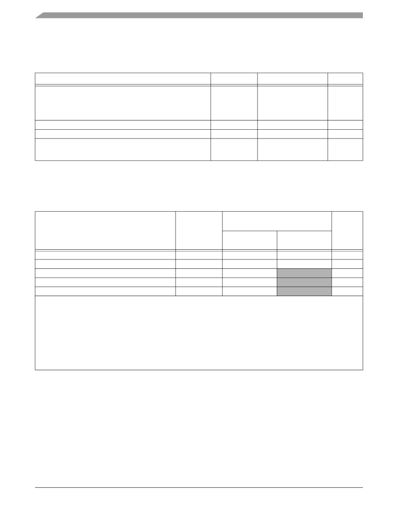
Table 3 lists recommended operating conditions. Proper device operation outside of these conditions is not guaranteed.
Table 3. Recommended Operating Conditions
Core and PLL supply voltage:
? Standard
— 400 MHz
— 500 MHz
? Reduced (300 and 400 MHz)
I/O supply voltage
Input voltage
Rating
Symbol
V DD
V CCSYN
V DDH
V IN
Value
1.14 to 1.26
1.16 to 1.24
1.07 to 1.13
3.135 to 3.465
–0.2 to V DDH +0.2
Unit
V
V
V
V
V
Operating temperature range:
? Standard
? Extended
T J
T J
0 to 90
–40 to 105
°C
°C
Table 4. Thermal Characteristics for the MSC8126
Characteristic
Symbol
FC-PBGA
20 × 20 mm 5
Natural
200 ft/min
Convection
(1 m/s) airflow
Unit
Junction-to-ambient, four-layer board
Junction-to-ambient 1, 2
Junction-to-board (bottom) 4
Junction-to-case 5
Junction-to-package-top 6
1, 3
R θ JA
R θ JA
R θ JB
R θ JC
Ψ JT
26
19
9
0.9
1
21
15
°C/W
°C/W
°C/W
°C/W
°C/W
Notes:
1.
2.
3.
4.
5.
6.
Junction temperature is a function of die size, on-chip power dissipation, package thermal resistance, mounting site (board)
temperature, ambient temperature, air flow, power dissipation of other components on the board, and board thermal
resistance.
Per SEMI G38-87 and JEDEC JESD51-2 with the single layer board horizontal.
Per JEDEC JESD51-6 with the board horizontal.
Thermal resistance between the die and the printed circuit board per JEDEC JESD 51-8. Board temperature is measured on
the top surface of the board near the package.
Thermal resistance between the die and the case top surface as measured by the cold plate method (MIL SPEC-883 Method
1012.1).
Thermal characterization parameter indicating the temperature difference between package top and the junction temperature
per JEDEC JESD51-2.
MSC8126 Quad Digital Signal Processor Data Sheet, Rev. 15
14
Freescale Semiconductor
发布紧急采购,3分钟左右您将得到回复。
相关PDF资料
MSC8144ADS
ADS FOR MSC8144 DEVICE
MSC8156EVM
EVAL MODULE FOR MSC8156 LC
MSL1060AW
IC LED DRIVER 6 STRING
MSL1061AV
IC LED DRIVER 6 STRING
MSL2041GU
IC LED DRIVER 4 STRING
MSL2100BR
IC LED DRIVER 8 STRING
MSL2160DQ
IC LED DRIVER 16 STRING
MSL2162DQ
IC LED DRIVER 16 STRING
相关代理商/技术参数
MSC8126MP8000
功能描述:DSP 16BIT 500MHZ MULTI 431FCPBGA RoHS:否 类别:集成电路 (IC) >> 嵌入式 - DSP(数字式信号处理器) 系列:StarCore 标准包装:40 系列:TMS320DM64x, DaVinci™ 类型:定点 接口:I²C,McASP,McBSP 时钟速率:400MHz 非易失内存:外部 芯片上RAM:160kB 电压 - 输入/输出:3.30V 电压 - 核心:1.20V 工作温度:0°C ~ 90°C 安装类型:表面贴装 封装/外壳:548-BBGA,FCBGA 供应商设备封装:548-FCBGA(27x27) 包装:托盘 配用:TMDSDMK642-0E-ND - DEVELPER KIT W/NTSC CAMERA296-23038-ND - DSP STARTER KIT FOR TMS320C6416296-23059-ND - FLASHBURN PORTING KIT296-23058-ND - EVAL MODULE FOR DM642TMDSDMK642-ND - DEVELOPER KIT W/NTSC CAMERA
MSC8126TMP6400
功能描述:DSP 16BIT 400MHZ MULTI 431FCPBGA RoHS:否 类别:集成电路 (IC) >> 嵌入式 - DSP(数字式信号处理器) 系列:StarCore 标准包装:2 系列:StarCore 类型:SC140 内核 接口:DSI,以太网,RS-232 时钟速率:400MHz 非易失内存:外部 芯片上RAM:1.436MB 电压 - 输入/输出:3.30V 电压 - 核心:1.20V 工作温度:-40°C ~ 105°C 安装类型:表面贴装 封装/外壳:431-BFBGA,FCBGA 供应商设备封装:431-FCPBGA(20x20) 包装:托盘
MSC8126TVT6400
功能描述:IC DSP QUAD 16B 400MHZ 431FCPBGA RoHS:是 类别:集成电路 (IC) >> 嵌入式 - DSP(数字式信号处理器) 系列:StarCore 标准包装:2 系列:StarCore 类型:SC140 内核 接口:DSI,以太网,RS-232 时钟速率:400MHz 非易失内存:外部 芯片上RAM:1.436MB 电压 - 输入/输出:3.30V 电压 - 核心:1.20V 工作温度:-40°C ~ 105°C 安装类型:表面贴装 封装/外壳:431-BFBGA,FCBGA 供应商设备封装:431-FCPBGA(20x20) 包装:托盘
MSC8126VT8000
功能描述:IC DSP QUAD 16B 500MHZ 431FCPBGA RoHS:是 类别:集成电路 (IC) >> 嵌入式 - DSP(数字式信号处理器) 系列:StarCore 标准包装:2 系列:StarCore 类型:SC140 内核 接口:DSI,以太网,RS-232 时钟速率:400MHz 非易失内存:外部 芯片上RAM:1.436MB 电压 - 输入/输出:3.30V 电压 - 核心:1.20V 工作温度:-40°C ~ 105°C 安装类型:表面贴装 封装/外壳:431-BFBGA,FCBGA 供应商设备封装:431-FCPBGA(20x20) 包装:托盘
MSC81325M
制造商:STMICROELECTRONICS 制造商全称:STMicroelectronics 功能描述:RF & MICROWAVE TRANSISTORS AVIONICS APPLICATIONS
MSC81350M
制造商:STMICROELECTRONICS 制造商全称:STMicroelectronics 功能描述:RF & MICROWAVE TRANSISTORS AVIONICS APPLICATIONS
MSC81400M
制造商:STMICROELECTRONICS 制造商全称:STMicroelectronics 功能描述:RF & MICROWAVE TRANSISTORS AVIONICS APPLICATIONS
MSC81402
制造商:STMICROELECTRONICS 制造商全称:STMicroelectronics 功能描述:RF & MICROWAVE TRANSISTORS GENERAL PURPOSE AMPLIFIERS APPLICATIONS
